深圳技术大学:超薄石墨烯应变传感器阵列,用于毫米级分辨率的高灵敏度多功能传感
石墨烯柔性传感器阵列的应用受两大限制制约:现有制备方法难以实现高空间分辨率,且缺乏面向实际应用的系统级集成方案。为应对这些挑战,本文,深圳技术大学贾原 副教授、天津师范大学王程 副教授、哈尔滨工业大学Hao Sun等研究人员在《ADVANCED SENSOR RESEARCH》期刊发表名为“Ultrathin Graphene Strain Sensor Arrays for High-Sensitivity Multifunctional Sensing with Millimeter-Scale Resolution”的论文,研究提出基于超薄石墨烯应变传感器阵列的全集成平台。该阵列采用化学气相沉积法生长的石墨烯与自上而下微加工技术,制备于5微米厚聚酰亚胺基板上。通过4×4布局与1mm单元间距设计,实现约64units cm−2的器件密度,从而达到毫米级空间分辨率。
该平台整合了完整的开发流程,涵盖传感器阵列制造、柔性电路设计、信号控制及数据采集。耐久性测试显示其在5000次弯曲循环中性能稳定。应变灵敏度测量表明,在0.8%应变下最大应变系数达144,动态测试则呈现0.2秒的快速响应时间与0.16秒的松弛时间。该平台可可靠解析局部压力分布、监测动脉脉搏波形并识别表面曲率,充分展现其多功能传感能力。这些成果证实了该平台在可穿戴健康监测、柔性机器人及新一代柔性电子设备领域的实际应用可行性。
2图文导读
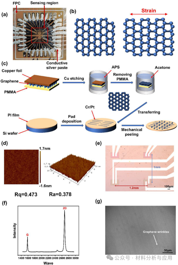
图1、Structure, sensing mechanism, and fabrication process of the sensor. a) The photograph of the strain sensor array; b) schematic illustration of the work mechanism; c) schematic illustration of sensor's fabrication process; d) 2D and 3D AFM micrograph of the PI film; e) microscopic image of the strain sensor array; e) Raman spectrum of the purchased CVD graphene; f) SEM micrograph of the purchased graphene.
图2、Data acquisition system. a) Photograph of custom DAQ and flexible printed circuit (FPC); b) schematic diagram of the Custom data acquisition (DAQ)board and the electrode lead-out (ELO) board; c) block diagram of the working principle of the main program in PC and sub program in the microcontroller.
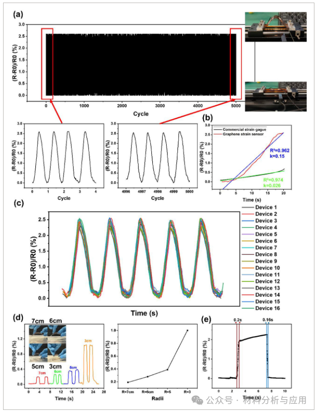
图3、a) Durability of the strain sensor in bending–release cycles, photograph inserted on the right showing the bending and flattening stage of the sensor; b) comparison of strain response between the strain sensor and a commercial metal strain gauge under identical test conditions; c) consistency inspection of 16 strain sensors; d) responses of the sensor to perse radii curvature; e) response/recovery times of the sensor.
图4、a) Photograph of testing and the radius measurement of the cylindrical object; b) schematic diagram of the row and column indexing of the sensor array; c) 3D bar charts of the sensor array responses to strain applied at six different regions, accompanied by schematic illustrations of the corresponding pressing points.
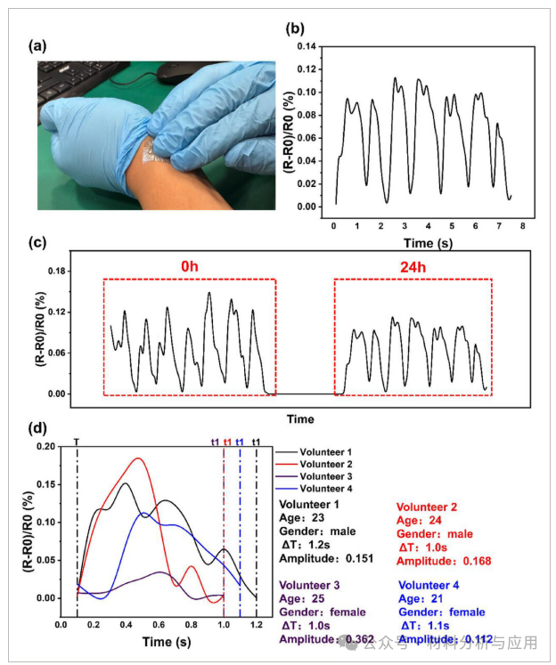
图5、a) The acquisition process of pulse waveforms; b) pulse waveforms detection results; c) comparison of pulse signals at seven random feature points before and after 24 h; d) pulse waveforms from four volunteers.
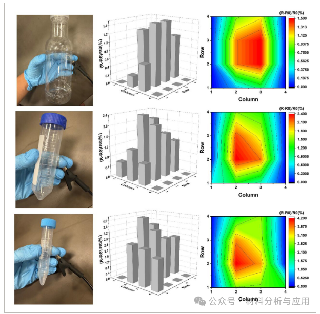
图6、3D bar charts and contour plots of sensor array responses to objects with different surface curvatures.
3小结
一种基于石墨烯的完全集成应变传感器阵列平台已在超薄聚酰亚胺基板上成功开发,实现了高空间分辨率、机械顺应性和应变灵敏度的理想组合。通过自上而下的微加工技术,将16个传感单元制备成0.5×0.5 cm²阵列,密度达≈64个器件/cm²。该阵列在5000次弯曲循环中表现稳定,并在0.8%应变下实现144的最大应变系数。局部载荷测试证实其具备毫米级分辨率且串扰极低。应用级验证包括脉搏波形监测与曲率微分测试,证实了该平台的多功能传感能力。这些成果凸显了超薄基板在提升机械适应性与传感精度的有效性。该平台为可穿戴电子设备、机器人皮肤及人机界面中的柔性传感提供了可扩展且可靠的解决方案。未来研究将聚焦阵列规模化与片上信号处理,以实现高吞吐量的智能触觉传感。
文献:
https://doi.org/10.1002/adsr.202500089
- 深圳技术大学:超薄石墨烯应变传感器阵列,用于毫米级分辨率的高灵敏度多功能传感
- 电力监控系统如何在智能变电站使用?
- 倾佳电子B3M010C075Z碳化硅MOSFET深度分析:性能基准与战略应用
- 能源新秘:耐达讯自动化Modbus RTU 转 Profibus 如何盘活智能水表?
- Quartus Prime Pro 25.1版本的安装和使用
- 串口以太网模块与三菱以太网通信处理器的 FX3U PLC - 触摸屏通讯应用案例
- 图扑数字孪生静态交通一网统管 | 智慧停车场合集
- 【有资料】开源CW32L011电机驱动器,硬件支持FOC
- ZWS云平台:储能经销商和终端业主的智能助手
- 倾佳电子代理的基本半导体驱动IC及电源IC产品力深度解析报告
- 东芝亮相2025上海国际电力元件和可再生能源管理展览会
- 推拉力测试机测试模块选择,看完选择不迷茫
- 加氢站和电力系统,谁是AEM产业化破局的关键?
- 翼辉软PLC方案的技术创新与实践
- AI安防选什么主板?杰和IB3-761靠“算力精准+多接口”出圈
- 信捷XS STUDIO编程软件V2.3.2版本的全新功能